Tsinghua releases a new Nature, achieving a new breakthrough in optoelectronic integration!
In 1965, Gordon Moore, one of the founders of Intel, proposed the "Moore's Law" that had influenced the chip industry for over half a century: it predicted that every about two years, the number of transistors that integrated circuits could accommodate would double. The semiconductor field has flourished and developed for decades, with "chips" becoming an important engine for humanity to enter the era of intelligence.
However, as the size of transistors approaches the physical limit, Moore's law has slowed down or even faced failure in the past decade. How to build a new generation of computing architecture and establish a "new" order for chips in the era of artificial intelligence has become a cutting-edge hot topic of high international attention.
In response to this challenge, Tsinghua University recently published its latest research findings in the world's top academic journal Nature. The news shows that the Department of Electronic Engineering at Tsinghua University (Associate Professor Fang Lu and Associate Researcher Qiao Fei) and the Department of Automation (Academician Dai Qionghai and Assistant Professor Wu Jiamin) have jointly researched and proposed a new computing architecture that goes beyond Moore's Law: an optoelectronic analog chip, with a computing power of over 3000 times that of current high-performance commercial chips.

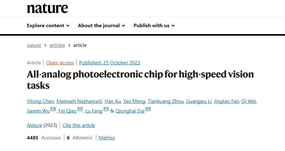
Image source: Screenshot of journal Nature
Optical computing, with its ultra-high parallelism and speed, is considered one of the most powerful competitive solutions for future disruptive computing architectures. The optoelectronic deep fusion computing framework proposed by the research team at Tsinghua University, starting from the most fundamental physical principles, combines optical computing based on electromagnetic wave spatial propagation with pure analog electronic computing based on Kirchhoff's law to break free from the physical bottleneck of the mutual constraints of data conversion speed, accuracy, and power consumption in traditional chip architectures, and break through large-scale computing unit integration, efficient nonlinearity Three international challenges for high-speed optoelectronic interfaces.

The Calculation Principle and Architecture of Optoelectronic Computing Chip ACCESS
Under actual measurement, the system level computing power of optoelectronic fusion chips has increased thousands of times compared to existing high-performance chip architectures.
However, such astonishing computing power is only one of the many advantages of this chip.
In the intelligent visual tasks and traffic scenario calculations demonstrated by the R&D team, the system level energy efficiency (the number of operations per unit energy) of the optoelectronic fusion chip has been measured to reach 74.8 Peta OPS/W, which is more than four million times that of existing high-performance chips. In terms of image, the electricity that originally provided one hour of operation for existing chips could provide it with over 500 years of operation.
A key factor currently limiting the limit of chip integration is the heat dissipation problem caused by high density. The optoelectronic fusion chip operating under ultra-low power consumption will greatly improve the chip's heating problem and bring a comprehensive breakthrough to the future design of the chip.
Furthermore, the minimum processing line width of the optical part of the chip is only at the level of one hundred nanometers, while the circuit part only uses the 180nm CMOS process, which has achieved multiple orders of magnitude of performance improvement compared to high-performance chips in the 7nm process. The materials used at the same time are simple and easy to obtain, and the cost is only a few tens of times that of the latter. It can be foreseen that with the continuous improvement of chip processing technology in China and the addition of more new materials in the future, what this article demonstrates is only the tip of the iceberg of this disruptive architecture potential.
The new architecture of optoelectronic fusion not only opens up a new path for this future technology to lead to daily life, but also deeply inspires the integration of other future efficient technologies such as quantum computing and in memory computing with current electronic information systems.
