Two New Breakthroughs in Chinese Scientists' Chips - Tsinghua's "Taiji II" and C
Recently, two teams of the Tsinghua Department and the Chinese Academy of Sciences in China have made major breakthroughs in new chips. The team of Tsinghua University has made further breakthroughs on the basis of the Taiji I optical chip released in April, and the Taiji - II optical chip was launched; The research team of the Chinese Academy of Sciences Shanghai Institute of Microsystems and Information Technology has developed a single crystal aluminum oxide gate dielectric material for two-dimensional integrated circuits, which can effectively prevent current leakage even when the thickness is only 1 nm.
Tsinghua's "Taiji II" optical chip has been launched
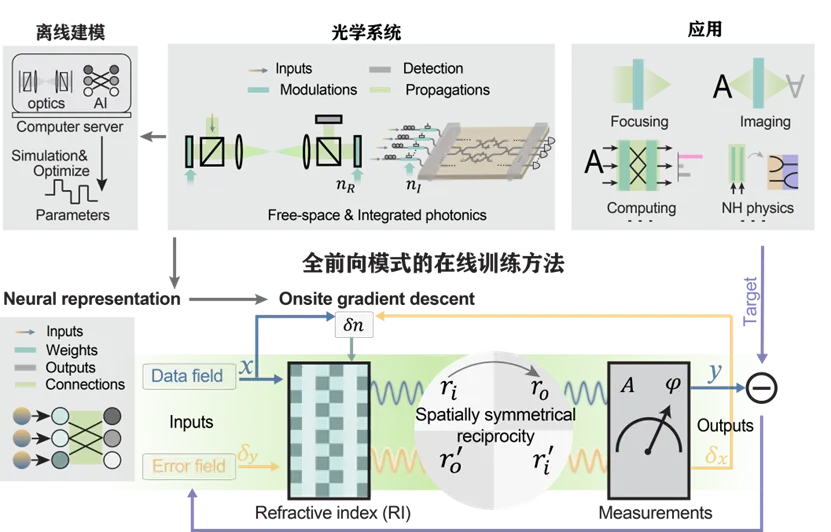
On August 8th, Tsinghua University announced that Professor Fang Lu's research group from the Department of Electronic Engineering and Academician Dai Qionghai's research group from the Department of Automation at Tsinghua University have pioneered a fully forward intelligent optical computing training architecture and developed the "Taiji II" optical training chip, achieving efficient and accurate training of large-scale neural networks in optical computing systems. The research findings, titled "Full Forward Training of Optical Neural Networks," were published online in the journal Nature on the evening of August 7th Beijing time.
In model training, existing optical neural network training heavily relies on GPU for offline modeling and requires precise alignment of physical systems, which greatly limits the scale of optical training and prevents the advantages of high-performance computing from being fully utilized. Faced with this dilemma, the research group led by Fang Lu and Dai Qionghai innovated the "Photon Propagation Symmetry" method, which equates the forward and backward propagation in neural network training to the forward propagation of light.
According to Xue Zhiwei, the first author of the paper and a doctoral student in the Department of Electronics, under the Taiji II architecture, the backpropagation in gradient descent is transformed into the forward propagation of the optical system. The training of the optical neural network can be achieved by using data error forward propagation twice. The two forward propagation have natural alignment characteristics, ensuring accurate calculation of physical gradients. The high training accuracy achieved in this way can support large-scale network training.

Full forward intelligent optical computing training architecture
Due to the absence of backpropagation, the Taiji II architecture no longer relies on electrical computing for offline modeling and training, allowing for precise and efficient optical training of large-scale neural networks.
The research in this paper shows that Taiji II can train various optical systems and demonstrate excellent performance in various tasks.
In the field of large-scale learning, the contradiction between computational accuracy and efficiency has been overcome, and the training speed of optical networks with millions of parameters has been increased by one order of magnitude. The accuracy of representative intelligent classification tasks has been improved by 40%.
Intelligent imaging of complex scenes: In low light environments (where the light intensity per pixel is only sub photons), all-optical processing with an energy efficiency of 5.40 × 10 ^ 6 TOPS/W has been achieved, resulting in a system level energy efficiency improvement of 6 orders of magnitude. Intelligent imaging with a kilohertz frame rate has been achieved in non visual field scenes, resulting in an efficiency improvement of 2 orders of magnitude.
In the field of topological photonics, non Hermitian outliers can be automatically searched without relying on any model priors, providing a new approach for efficient and accurate analysis of complex topological systems.
The Taiji I released in April this year has an area efficiency of 879 T MACS/mm2 and an energy efficiency of 160 TOPS/W, empowering light computing for the first time to achieve complex artificial intelligence tasks such as recognizing thousands of objects in natural scenes and generating cross modal content. The launch of Taiji II is a major breakthrough after Taiji I chip, further revealing the enormous potential of intelligent optical computing. If the two instruments are separated, Tai Chi I and II have respectively achieved high-efficiency AI reasoning and training; Similarly, the harmony of two instruments, Taiji I and II, together constitute the complete lifecycle of large-scale intelligent computing.
Based on the principle sample, the research team is actively moving towards the industrialization of intelligent optical chips and has deployed applications on various end side intelligent systems. The intelligent light computing platform is expected to open up new paths for high-speed and energy-efficient computing of artificial intelligence models, general artificial intelligence, and complex intelligent systems with lower resource consumption and lower marginal costs.
Chinese Academy of Sciences team develops insulation material for new chips
As the basic components that make up a chip, the size of the transistor gradually approaches its physical limit as the chip shrinks, and the gate dielectric material that plays an insulating role is crucial.
Recently, the team of Di Zengfeng, a researcher at the Chinese Academy of Sciences Shanghai Institute of Microsystems and Information Technology, developed a single crystal aluminum oxide gate dielectric material for two-dimensional integrated circuits - synthetic sapphire. This material has excellent insulation performance, and can effectively prevent current leakage even when the thickness is only 1 nm. The research team has published a research paper titled "Single crystalline metal oxide dielectrics for top gate 2D transistors" in the journal Nature. Dr. Zeng Daobing, a member of the team, is the first author of the paper, and researchers Tian Ziao and Di Zengfeng are co corresponding authors of the paper.

Di Zengfeng stated that two-dimensional integrated circuits are a new type of chip constructed from two-dimensional semiconductor materials with a thickness of only one or a few atomic layers, which is expected to break through the physical limits of traditional chips. However, due to the lack of high-quality gate dielectric materials that match it, there is still a significant difference between its actual performance and theory.
When the thickness of traditional gate dielectric materials is reduced to the nanometer level, the insulation performance will decrease, leading to current leakage and increasing the energy consumption and heat generation of the chip. To address this challenge, the team has innovatively developed in-situ intercalation oxidation technology.
The core of in-situ intercalation oxidation technology lies in precisely controlling the ordered embedding of oxygen atoms layer by layer into the lattice of metal elements. Traditional alumina materials usually have a disordered structure, which can significantly reduce their insulation performance at extremely thin layers. Tian Ziao, a researcher at the Chinese Academy of Sciences Shanghai Institute of Microsystems and Information Technology, said.
Specifically, the team first used germanium based graphene wafers as pre deposited substrates to grow single crystal aluminum metal. By utilizing the weak van der Waals forces between graphene and single crystal aluminum metal, they achieved non-destructive exfoliation of 4-inch single crystal aluminum metal wafers. After exfoliation, the surface of the single crystal aluminum metal exhibited defect free atomic level flatness. Subsequently, in an extremely low oxygen atmosphere, oxygen atoms are embedded layer by layer into the lattice on the surface of single crystal aluminum metal, ultimately resulting in stable, accurately stoichiometric, and uniformly thick aluminum oxide thin film wafers at the atomic level.
Di Zengfeng introduced that the team has successfully prepared a low-power transistor array using single crystal alumina as the gate dielectric material, and the transistor array has good performance consistency. The breakdown field strength, gate leakage current, interface state density and other indicators of transistors meet the requirements of the international device and system roadmap for future low-power chips, which is expected to inspire the development of a new generation of gate dielectric materials in the industry.
